

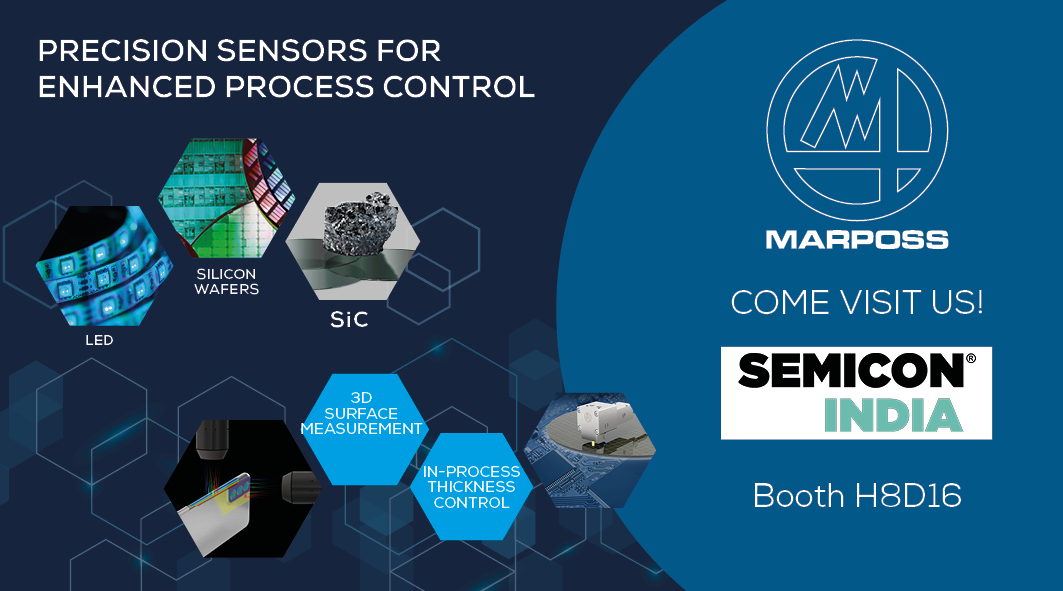
THE @MARPOSS GROUP STRENGTHENS ITS PRESENCE IN SEMICONDUCTOR AND CONSUMER ELECTRONICS SEGMENT ALSO. Placing and maintaining a process under control is the key factor for any production. This is even more true for the very demanding semiconductor and semiconductor like manufacturing processes, which can be considered some of the most complex ones, that requires the control of an increasing number of parameters. Not to forget that semiconductor is a brittle and hard material that requires dedicated machine tools to slice, lap, thin, get intelligent and finally cut the die.
In order to improve and maintain high yield, inspection and metrology are key factors. They are also crucial for the management of the semiconductor manufacturing process to find defects on both patterned and unpatterned wafers.
Marposs engineers are ready to support you in defining how to improve the performances of automatic machines used during wafer processing, the front-end and back-end fabrication steps. Indeed, we offer sensors and gauges for slicing and lapping machines, back grinders and dicing saws, wafer shape (bow/warp) measurements, layer & pattern measurements, bump & groove measurements.
The semiconductor and semiconductor like industries continue to produce ever smaller devices that are more complex in both shape and materials. For these purposes, Marposs has a complete range of non-contact sensors used for thin-film metrology, wafer dimensional characterization, wafer inspection and packaging inspection. Our sensors can work inside automatic inspection machines to find defects and dimensional variation.
Here some examples of how our products that can be of profitable used.
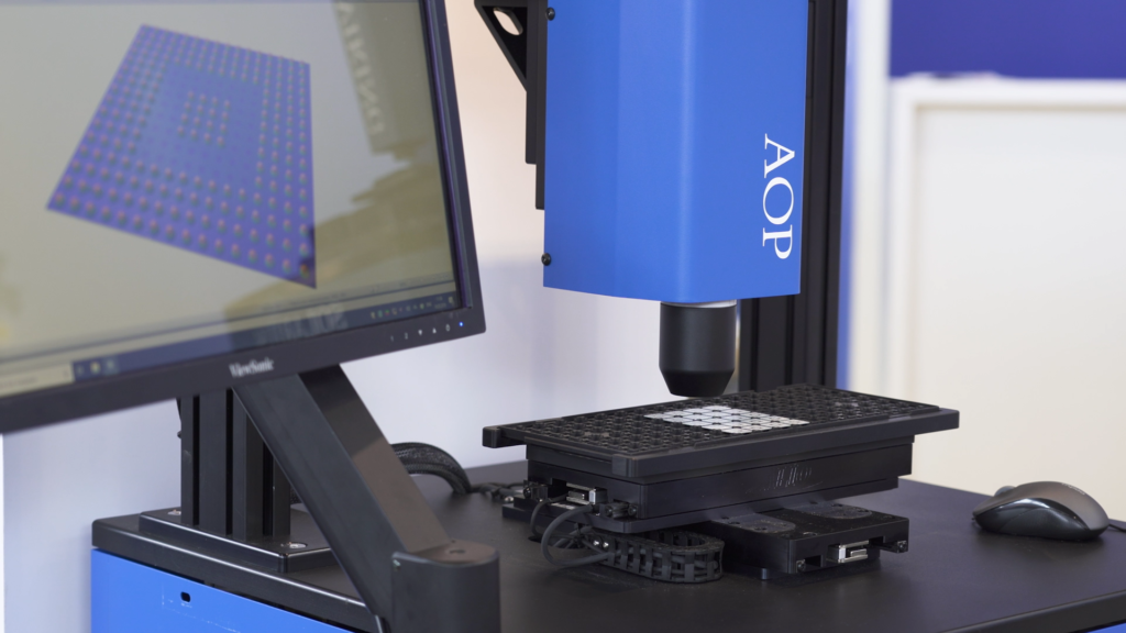
1-Solarius
Marposs already announced the acquisition of Solarius Development Inc., a leading provider of high-tech manufacturing solutions for the Consumer Electronics and Semiconductor Industry.
The new Phoenix Desktop 3D surface measuring system from Solarius enables highly accuracy and precise 3D surface inspection. Phoenix expands the scope of application due to its extensive equipment, which supports in particular simple automation of the measurement tasks.
Phoenix Desktop 3D system is based on the Chromatic confocal technique dedicated to industrial environment, independent from ambient light Sub-micrometric accuracy & nanometric Axial resolution. In the design and calculation of the optics, great importance was attached to a physically optimal direction limitation of the optics, which allows for accurate, precise and repeatable lateral measurements.
Phoenix features a comfortable and precise automated X/Y positioning unit with 150mm x 150mm travel range and a height measuring range of 100m. The height measuring range can be adjusted up to 150mm in height using an accurate, manual traversing unit. Phoenix has six available sensors types with sensor head 45, 90 or 180 points of measure available which designed to meet the metrology require in mechanics, semiconductors, 3C, Glass, Automotive, Aerospace, Medical.
2-NCG Thin Line
NCG is a distance/thickness measurement system based on interferometric technology: waves, which are reflected at the layer boundaries of different surfaces (two or even more in case of multilayer material) of the object being measured, are brought to interference and the layer thickness is then calculated. The gauge has been designed to control the thickness of parts of different materials such as for instance silicon, doped silicon, SiC, Sapphire, GaN, Glass, GaAs, SOI, plastic and so on. Thanks to the infrared light sources is possible to measure non-transparent materials too. NCG can be equipped with different light emitters that covers mutliple thickness range for each material, down to a lower limit of few microns. A wide range of interferometric probes is available to fit both measurement performed in clean environment but also in the harsh condition typical of machine tools.
NCG is also equipped with a powerful measure elaboration SW able to provide a ‘clean’ measurement even in an optical noisy environment and also to efficiently track the measure of each single layer in case of multilayer materials that can be easily confused each other.
NCG can be used and programmed thorugh a dedicated human interface that suites for all offline applications. Moreover, measurement carried out by NCG can be forwarded to other machines (Machine Tools, Complex Measuring Benches or similar), through different protocols that are provided with special SW package together with the electronic unit.
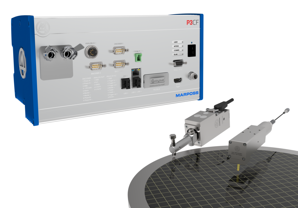
3-P3CF + Unimar
P3CF is a high precision measurement system that combines chromatic confocal with touch measurement technology. The confocal probe is connected to the controller via a fibre optic cable. Different confocal probe models are available to fit both measurement performed in clean environment but also in the harsh condition typical of machine tools. Contact probes belongs to the UNIMAR family week know for its versatility and reliability in any kind of machining.
P3CF if the ideal solution where it is necessary to provide an indirect thickness meaurement. When direct thickness measurement is not possible cause the material cannot be penetrated by standard NIR (Near InfraRed) waves, thickness of target can be measured getting the distance of the target through the confocal probe (avoiding to touch it) and subtract the distance of the support of the target detected with standard UNIMAR (support is usually tough and often does not have good light reflectance, so contact probe is the perfect solution).
P3CF can be used and programmed thorugh a dedicated human interface that suites for all offline applications
Moreover, measurement carried out by P3CF can be forwarded to other machines (Machine Tools, Complex Measuring Benches or similar), through different protocols that are provided with special SW package together with the electronic unit. For high-level integration in factory network the system supports also most commont types of Fieldbus.
Discover more about Marposs solutions for the semiconductor industry and visit http://www.stilsa.com/ For More Details you can also Call Marposs in India – 0124 473 5776/765 or e-mail to Sales@in.marposs.com